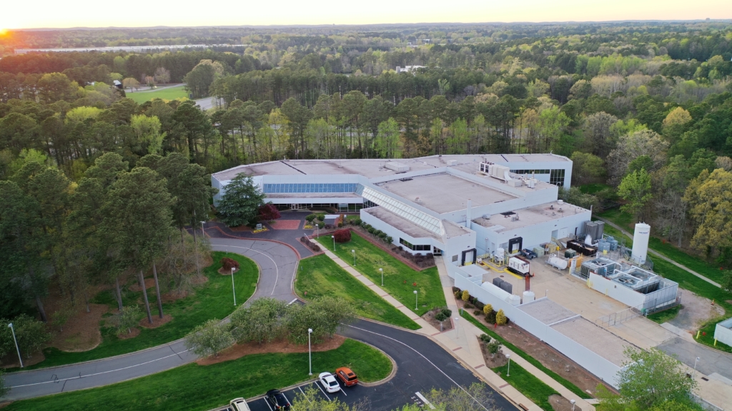
Micross AIT

Micross Advanced Interconnect Technology (Micross AIT) is home to one of the premier wafer bumping and wafer level packaging facilities in the U.S., with 30+ years of experience in developing and providing leading edge interconnect and integration technologies to customers around the world. We have the unique ability to support early stage development needs as well as volume production for more mature applications. Our ITAR Registered facility supports wafer sizes from 100mm – 300mm with established and proven WLP processes and the flexibility to tailor unique solutions for your most demanding advanced packaging and 3D integration solutions that enable higher-performance systems with decreased size, weight, and power (SWaP).

